4.3 Implementation
The figures come from the Vivado 2022.1 post-route implementation of the U280 board build (make u280, RS-FEC on): the SINGLE core with one port and four 280-bit Kulisch banks, without the FP32 arrival path, behind the CMAC subsystem and packet adapter of the OpenNIC shell (see prism_u280_top).
Timing
Every path meets the 4 ns period of the 250 MHz clock: worst setup slack +0.005 ns, worst hold slack 0.000 ns, and no failing endpoint among 1.23 million. The RS-FEC-off build closes with +0.010 ns. Both bitstreams are attached to the v1.0.0 release.
Placement
The U280 is built from three dies, or super logic regions (SLRs). The design fills SLR1 and SLR2; SLR0, next to the HBM, stays empty. The output path, which classifies results, forms the AUTO groups, and writes RESULT frames, covers most of both dies. Signals between SLR1 and SLR2 use 13,984 of the 23,040 links across that boundary (61%).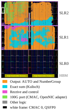
Utilization
| Resource | Board build | Core | Device | SLR1 | SLR2 |
|---|---|---|---|---|---|
| CLB LUTs | 529,840 | 519,855 | 40.64% | 62.95% | 59.70% |
| CLB registers | 542,583 | 508,849 | 20.81% | 38.78% | 24.02% |
| BRAM tiles | 281 | 263.5 | 13.94% | 38.10% | 3.72% |
| DSPs | 2 | 2 | 0.02% | 0.07% | 0.00% |
The output path uses 68% of the LUTs, the exact arithmetic (banks and final rounding) 26%, reception and control 3%, and the CMAC subsystem with the packet adapter about 10,000 LUTs, or 2%.
Power
Vivado's vectorless estimate of on-chip power is 13.6 W: 10.2 W dynamic and 3.4 W static, at a junction temperature of 30.9 °C. The core accounts for 6.7 W and the 100G port for 3.5 W, 2.3 W of which go to its four 25 Gbit/s transceivers. Clock distribution alone costs 3.8 W, more than the CLB logic (0.9 W).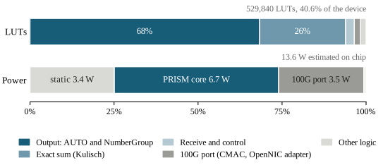
Scope and limits
- These figures describe the board build; the two-port performance simulations use a different configuration, and the line rate of this profile is measured separately. The 280-bit arithmetic-bank width also differs from the 320-bit serialized Kulisch representation used in the traffic comparison.
- Timing closes with little margin: a small change of the design or of the flow can leave a full build short of it (see Alveo U280).
- Two ports pass the same rate tests in simulation, but need 687,220 LUTs after synthesis, and their readout crosses the SLR boundaries more often than the 23,040 links allow. The readout has to change before two ports can be placed.
- An area comparison with an equivalent FP32 profile is still missing.
- The thesis as deposited reports an earlier revision of the standalone core, at 682,704 LUTs (52.37%).
Throughput, response time and power on the card itself are part of the hardware work. Report SHA-256 (Report provenance
post_route_physopt/utilization.rpt, utilization_hierarchical.rpt and timing_summary.rpt in the output directory of the build that produced the published RS-FEC-on bitstream, dated 15 October 2026; power from report_power on its routed checkpoint. The numbers, the Vivado screenshot and the plotting script are in experiments/05-experiment-u280-release/.utilization.rpt): 0071bef0b4fd6ee179a55f3f5ba67ec26861b72179dfd45d1b7e7d37eeadf066.